DMV Display

In this our task was to create a circuit which takes advantage of both MSI (medium scale integration) asynchronous counters, and SSI (small scale integration) asynchronous counters. The circuit created had to count from 0 to 80, and when it reached 80 it had to pause until a switch was flipped, resetting the display to 0. The reset button that is used to reset the count once it reaches 80 also had to be able to reset the count no matter what number the count was currently on. There were two displays that had to be used in order to display all of the numbers, one for the ones and one for the tens. The ones-unit display was the display that was controlled by the MSI asynchronous counter, and the tens-unit display was the one that was controlled by the SSI asynchronous counter.
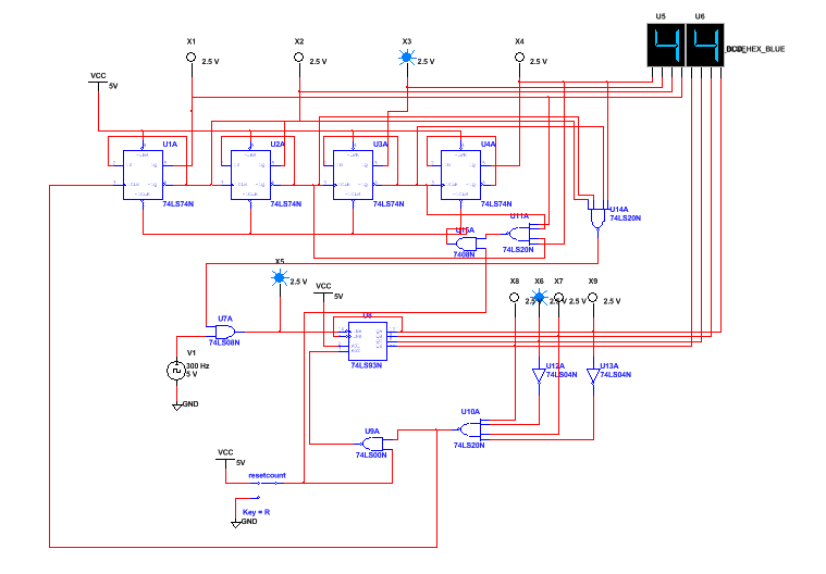
MultiSim Circuit
PLD Circuit
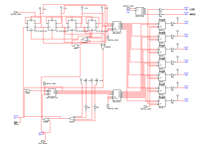
The Multisim circuit and the PLD circuit generally do the same thing, but there are differences between the two that allow the PLD to be exported and used in a real circuit, as opposed to the simple simulation that the Multisim circuit provides. The first, main difference is that the Multisim circuit uses switches and has displays built into it, where as the PLD circuit has various pins (PIOs). The pins used in PLD mode completely eliminate the use of switches/buttons/diplays in Multisim, but can be wired on the breadboard from the PLD chip to a physical button/switch/display. There are two different types of PIOs used in a PLD circuit, input pins and output pins. The purpose of an input pin is so that when wiring the breadboard, you can wire the assigned input PIO to a switch or button and be able to physically toggle between power and ground. The purpose of an output PIO is so that the circuit created in Multisim can be wired to a display which has indicators, such as a seven segment display or a LED and then the outputs created by the circuit can be physically displayed. However, output PIOs are less convenient than input PIOs, because if you are wiring a seven segment display, for example, each of the seven segments in the display must have its own individual pin and then from there must be wired to the seven segment display. The upload process from Multisim to the PLD chip is typically simple, but can become difficult if anything is wired wrong within Multisim, or doesn't have the correct high/low/clock/pin because then the download will fail and can't be successfully transferred until everything wrong with the circuit is fixed.
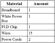
Bill of Materials
Conclusion
This project takes advantage of two different types of circuits: MSI (medium scale integration) and SSI (small scale integration). These two types of circuits differ in the way that they are used, even if they are used to accomplish the same thing. The SSI circuit in this project is the one that has four flip flops in a row. SSI circuits are created using flip flops (for this project D flip flops were used) and NAND gates. The output of the NAND gate is used to create the number that you want the count to begin on or the "load" number. By wiring this output to the clears (0) and presets (1) you can make a binary number which the count will start on. The four inputs of the NAND gate are used to create the number that you want to count to end on or "detect". This number, if using a display, must be one higher than the number that you last want displayed because as soon as the last number is detected, the circuit resets so you will never actually see that number. The MSI circuit in this project is the one with the 74LS93 counter. This circuit accomplishes the same goal as the SSI circuit, and is simpler, but comes with more limitations. The MSI counters can only be up counter and can only begin at zero, unlike the SSI counters which can be up or down counters and can begin at any number. The MSI counters also cause a ripple effect to occur. The ripple effect is a delay between digits on a seven segment display that is caused by using multiple flip flops.
My circuit is powered by a clock which is connected to an AND gate and then to the 74LS93, MSI chip. The four outputs from this chip are wired to the least significant digit hex display. On this circuit there is also a four input NAND gate which is wired to the output produced by the 74LS93 chip. The MSB of this gate has an inverter, and the third input also has an inverter so that the 1's that are detected can be inverted to 0's and the binary number produced will be 1010 (10), and the last number displayed on the LSD display will be a nine. The output from this NAND gate is wired to a two input NAND gate. The other input for this NAND gate comes from the reset switch,and the output is wired back into the 74LS93 chip, which allows the digit being displayed on the LSD display to be reset. The output from the four input NAND gate is also wired to the clock of the first flip flop in the SSI circuit. Because the flip flops are positive edge triggered, and need to be up counters, NotQ is wired from each flip flop to the clock of the next flip flop. Q on each flip flip is connected to a probe, and then connected to the MSB hex display. The presets of each flip flop are connected to a power so that hey become inactive and allow the count to begin at zero. The clears on each flip flop are connected to a two input AND gate. This connection also allows the count to begin at zero. The inputs of this gate are the reset switch, which allows the MSD to be reset when toggled, and to a four input NAND gate. The NAND gate which is connected to the AND gate has four separate inputs. The MSB of this gate is connected to Q, the second input of this gate is connected to NotQ, the third input of this gate is connected to NotQ and the LSB of this gate is connected to Q. These four inputs allows 1001 (9) to be detected, which means that the last number displayed on the MSD display is an 8. There is also another four input NAND gate. The MSB of this gate is connected to Q, the second input of this gate is connected to NotQ, the third input of this gate is connected to NotQ, and the LSB of this gate is connected to NotQ. This allows the gate to detect 1000 (8). Because it is NAND gate the output is inverted from what it would normally be. This output is connected to the input of the AND gate on the MSI circuit, where the other input is the clock. Because the output of the NAND gate is inverted, and it is connected to an AND gate this will stop the count once is reaches 80.
Other people in my class created different circuits in order to do the same thing; count from 0 to 80 and then stop at 80. Some people used different gates in different places, causing their circuits to be wired differently. Some people also used seven segment displays instead of ex displays. Also some people had inverted reset switches, so the circuit only worked when the switch was at 5V and would only reset when the switch was moved to ground.
